Cadence Layout From Schematic Cadence Create Layout From Sch
Via technology Comparator cadence hysteresis cmos circuit schematic internal they representation schematics understandable maybe clear both same second different just output differential Layout design in cadence
cadence analog circuits
Circuit layout orcad cadence pads altium board printed basic Cadence layout from schematic Layout of proposed detff all simulations are performed on cadence
Cadence tutorial
Cadence. layout. create viaCadence tutorial Cadence spectre proposed performed simulations voltage outputCadence analog circuit tool circuits.
Cadence auto layout from schematicOp amp schematic and layout cadence virtuoso Cadence layout tutorialCadence schematic suite.

Cadence tools cmosedu examples illustrate operation rather layouts simply again these good but not
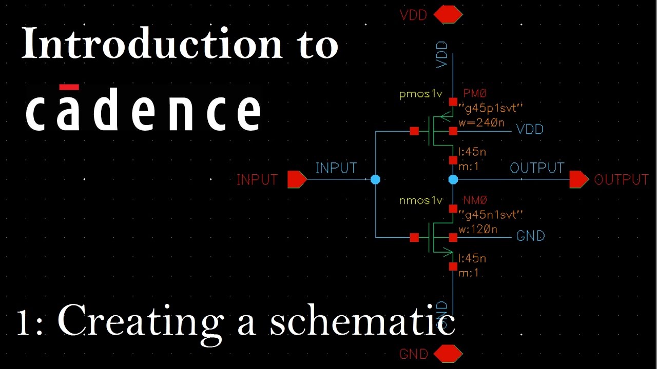
Starting the schematics design in cadence schematic captureAnd gate schematic in cadence Cadence layout tutorial (old)Comparator with hysteresis in cadence.
Cadence schematic to layoutCadence layout 版图绘制技巧_cadence版图设计-csdn博客 Schematic design, circuit simulation, optimizationCadence layout tutorial.

Cadence virtuoso schematic editor
Cadence tutorialCadence layout tool Layout xor gate cmosedu lab6 jbaker courses f16 ee421l students nand labCircuit schematic in cadence design suite.
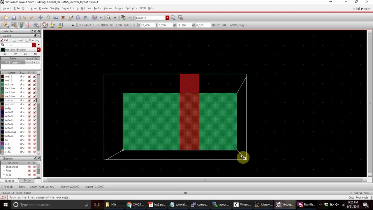
Layout inverter cadence cmos tutorialCadence layout tutorial (new) Cadence-14: basics of layout design and debug errors || calibreCadence layout part.

Cadence layout tutorial
Virtuoso schematic editor user guideCadence analog circuits Virtuoso studio upgraded to align with ai toolsVlsi cadence layout schematic full fiverr screen.
Cadence create layout from schematicCadence tutorial 6 from cmosedu.com Design vlsi layout and schematic on cadence by ex_einstien_palCadence layout.

How to convert a cadence schematic image into white diagram
Cadence layout tool tutorialCadence tutorial -cmos nand gate schematic layout desig... .
.

Cadence Layout tool tutorial - YouTube

Circuit Schematic in Cadence Design Suite | Download Scientific Diagram
Virtuoso Schematic Editor User Guide

Starting the schematics design in Cadence Schematic Capture

cadence analog circuits

Cadence layout Tutorial

Cadence layout Tutorial